
Nowadays, when technology has taken primacy, we can hardly imagine life without devices such as TVs, computers and the like. Have you ever thought about what components are necessary to ensure that they work properly? A PCB – or printed circuit board is one such component. These components are essential for the operation of many devices that we use almost daily. And how they are made, what they serve and what is the difference between single-layer and multi-layer PCBs – we will try to explain below.
What is PCB?
The problem of designing electronic devices dates back to the beginning of the 20th century. Back then, a serious engineering discipline was developed – in which systematically studied methods and techniques for making electronic devices. The design of modern electronic devices is almost always based on drawing and making a printed circuit board that is the foundation of almost every electronic device. Such a printed circuit board or PCB is a physical component carrier in the unit. It also provides electrical connectivity for the other components in the circuit. The process of constructing it requires the designer to know all the disciplines necessary for the design of the electronic circuit.
Design And Production Of Printed Circuit Boards
The design and manufacture of printed circuit boards are of particular importance for the design of modern electronic devices. The printed circuit board connects the components of the device to the functional circuit – bringing its electrical properties into it, but also forms mechanical support that holds the entire structural structure connected. It can be said that this is the physical and electrical basis of every device, which, like all other components, is unfortunately subject to key criteria – the cost of production. For this reason, such boards must be cheap to produce, easy to assemble, and reliable enough not to compromise the integrity of the device. When we add these electrical requirements to those of miniaturization – it becomes clear why PCB design may be the most important step in the designing process.
What Does A Printed Circuit Board Look Like?
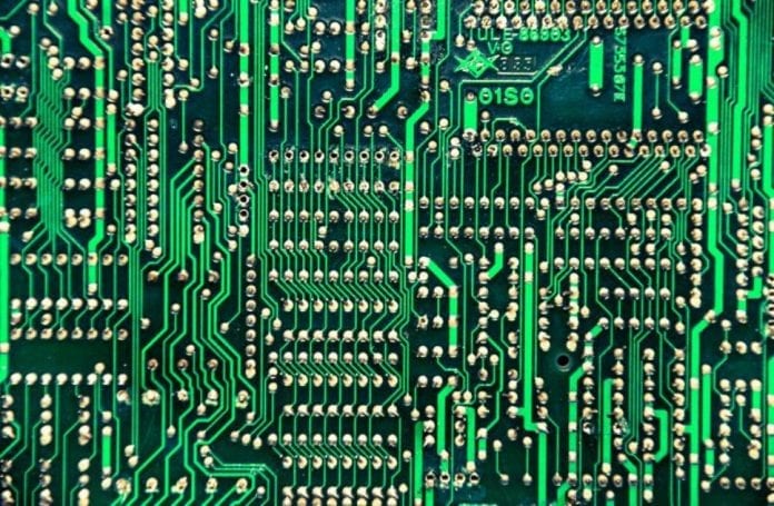
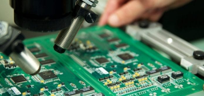
In short, the printed circuit board is an insulating material of good mechanical quality, on whose surface, usually made of copper – the conductors are formed. That way, it is connecting components in an electronic circuit. The process of designing a printed circuit board involves the step of drawing a scheme according to a circuit model with concentrated parameters and the process of drawing the printed circuit board takes place in two-dimensional projection. Some modern print design programs allow you to view drawn prints in three dimensions, with 3D component models – but do not allow drawing lines in three dimensions.
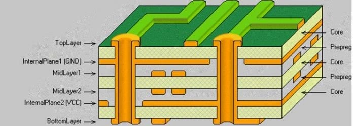
What Are Multilayer PCBs?
The main products of this type include one-sided, double and multilayer circuit boards. The one-sided board is the simplest one. Its components are focused on one side – while wires are relatively set on the other side. Double-sided – refers to wiring on both sides. This way it is corresponding connections between the two sides. It usually solves some issues of interconnecting wiring with one-sided boards. However, according to PCBOnline, they can be used on some more complex circuits. A multilayer PCB means boards with multiple conductive samples. The interesting fact is that the number of layers on such boards is usually an even number. The more layers – the higher the technical requirements are. Therefore, more functions will be able to support it.
How Are They Produced?
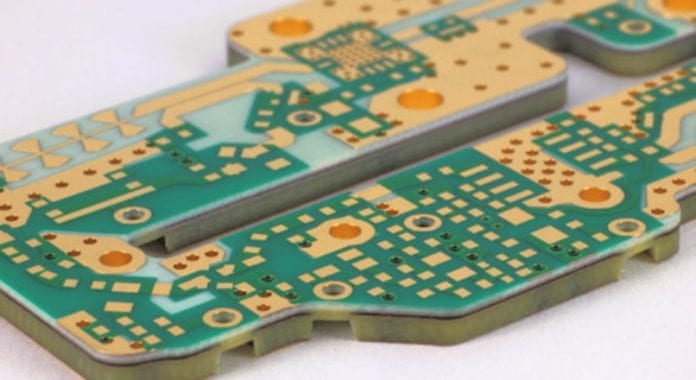
A multi-layer board is composed of two or more layers – interconnected by a resin layer. This design process is a relatively complicated one. Its layers are laminated and afterward exposed to high temperatures and pressure. It is a regular process of producing such boards. This process is ensuring that no air is trapped between any of the existing layers. All the conductors are sealed with resin. The materials range used for this purpose varies from epoxy glass to various ceramic or Teflon. Afterward, they are set into the lamination printer. Exposed to high temperatures and pressure – the material melts causing the connection between the layers. After it cools down – we will have a brand new, solid circuit board.
The Application
In today’s advanced technology, production and application of multilayer printed circuit boards is highly developed. They are used in many industries, and therefore have a great impact on the market. There are many reasons for that.
Small Dimensions
With the development of modern technology and modern devices that have taken on smaller dimensions – it is logical that miniaturization of circuit boards is also flourishing. Namely, since these panels are a basic component of some devices of very small dimensions, it is quite clear that they themselves have undergone a reduction to some almost microscopic dimensions. What is expected is that in the near future, by further processing their dimension, it will reach a size of only four millimeters.
Better Functionality
This technology already allows not only smaller dimensions but also far thinner panels. This further benefits the functionality of the products in which the PCBs have been implemented. We can almost say with certainty that consumer electronic equipment is the main initiator of circuit board production. With increasing interest in functional devices, the demand for PCBs has grown.
Use In Medicine

The development of technology in medicine also affects the increased use of PCB-enabled devices. In modern times, medical diagnostics is very advanced thanks to the devices that include the PCB. Some of the most commonly used type devices are camera probes that can be swallowed or otherwise inserted inside our bodies. Therefore, it will be easier for doctors to diagnose the disease we are suffering from. And all this would not be functional if there were no circuit boards that are an integral part of these devices.
Monitoring
This technology is also very important in security measures. Specifically, various monitoring devices such as cameras are often used. Not only does their application today apply to security institutions – but it is also very commonly used in everyday life. For example – many of us use a security camera in front of the house or inside our homes. This way, PCB has proven again to be extremely useful because each of these devices has such boards in their basic structure.


